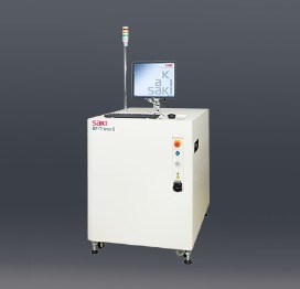
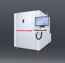
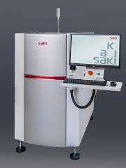
No need to flip the board! Bottom-side inspection machine that enhances line productivity
.png)
Ensures quality and productivity by eliminating the need for manual operation and board flipping.
2Di-LU1's Feature
Saki’s unique Line Scan technology
|
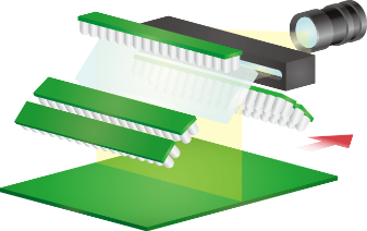
Saki’s unique Line Scan imaging technology is applied to bottom-side inspection. High-speed imaging enables inspection of large PCBs in one pass in about 9 seconds. This production is compatible with large odd-shaped inserted component mounted-PCBs and heavy jigs.
|
|
 |
|
Bottom-side scanning
|
"What is Saki's Line Scan Technology?"
 |
|
Saki 2D AOI systems use a unique line-array CCD camera to capture the entire PCB image for each inspection. The speed of image capture is unaffected by the number of components on the PCB, as is the case with conventional FOV-type AOI systems. Saki's Line Scan Technology is the backbone of our 2D AOI systems, producing accurate and reliable inspection data at high speeds.
|
Inspection algorithms that accurately determine defects
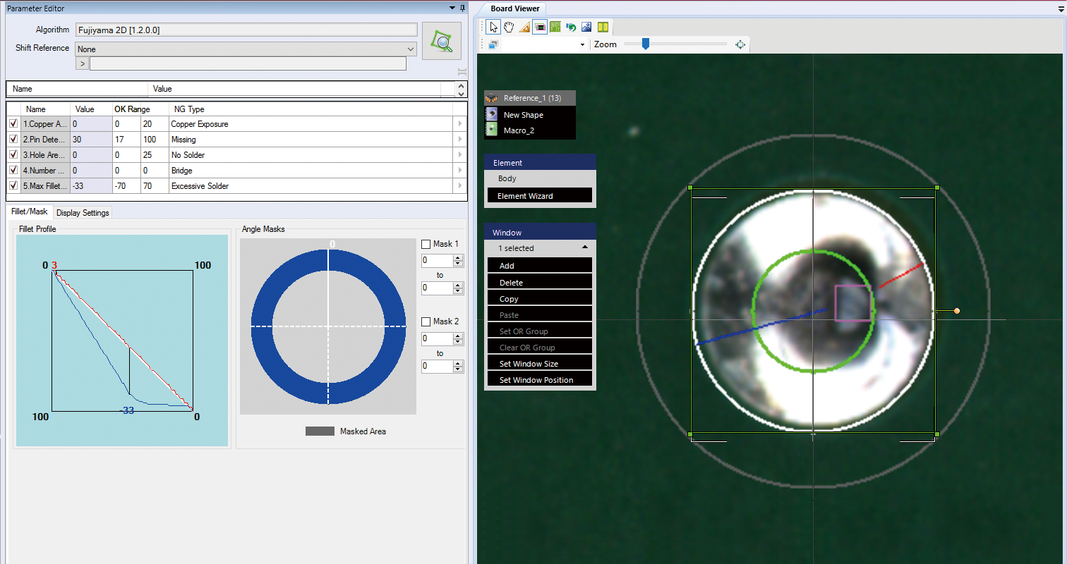
THT solder inspection "FUJIYAMA" algorithm
|
By analyzing solder meniscus and pin presence using Saki’s unique lighting technology, the following defects are simultaneously inspected:
• Copper exposure • Excessive solder
• Pin presence • Insufficient solder
• Blow holes • Solder bridges
|
|
 |
|
FUJIYAMA user interface
|
Extra Component Detection (ECD) inspection capability
|
Utilizing Saki’s technology that scans the entire PCB in one pass, it is possible to detect abnormalities such as dropped chip parts and solder balls in the entire board at the same time as normal solder inspection. An average OK image is generated from several images of non-defective boards and compared with the inspection target to automatically detect defects.
|
|
 |
|
ECD inspection window
|
Software design that can be linked with the SMT inspection process
|
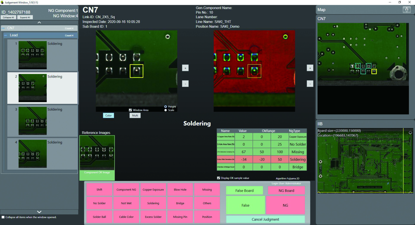
It uses the same software platform as the 3D Solder Paste Inspection machine (SPI) and 3D Automated Optical Inspection machine (AOI) systems.
Additionally, by using the same system options as Saki’s SPI and AOI solutions, the operator’s workload is reduced.
|
|
 |
|
Software operation screen
|
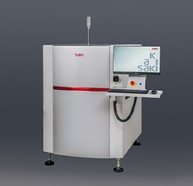
Specifications
Dimensions
(W) x (D) x (H) [Main body]mm (in.) |
1040 x 1440 x 1500
(40.94 x 56.69 x 59.06) |
| Weight |
Approx. 750 Kg (1653.47 lbs) |
| Electric Power Requirement |
Single-phase ~ 200-240V +/-10%, 50/60Hz, 700VA |
| Resolution |
18μm |
| Air Requirement |
0.5MPa, 5L/min (ANR) |
Target PCB Size
mm (in.) |
Carrier
50 W x 60 L - 610 W x 610 L
(1.97 W x 2.36 L – 24.02 W x 24.02 L)
Inspection area (Scan)
50 W x 60 L - 460 W x 500 L
(1.97 W x 2.36 L – 18.11 W x 19.69 L) |
| PCB Clearance |
Top: 130mm (5.12 in.)
Bottom: 40mm (1.57 in.) |

.png)

