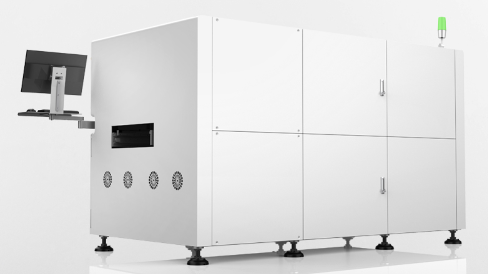
KLA Corporation has announced the launch of its revolutionary Axion T2000 X-ray metrology system for advanced memory chip manufacturers. Fabrication of 3D NAND and DRAM chips involves precise formation of extremely tall structures with deep, narrow holes and trenches, and other intricate architectural shapes – all requiring control at the nanoscale level. The Axion T2000 features patented technologies that power its ability to measure high aspect ratio device features with an unprecedented combination of resolution, accuracy, precision and speed. By discovering the small shape anomalies that can impact memory chip performance, the Axion T2000 helps ensure successful production of the memory chips used in applications such as 5G, artificial intelligence (AI), data centers and edge computing.
.jpg)
“Our new Axion T2000 X-ray metrology system is a game changer for inline process control during fabrication of advanced 3D NAND and DRAM devices,” said Ahmad Khan, president of the Semiconductor Process Control business unit at KLA. “Using transmissive X-ray technology, the Axion T2000 quickly generates a complete 3D visualization of high aspect ratio structures on the order of 100:1 or greater. From the top to the very bottom of these extreme vertical features, Axion data facilitates tight control of critical parameters, such as width, shape and tilt. Moreover, by measuring inline, the Axion reduces the cycle time required to solve critical yield and reliability issues during high volume production of memory chips.”
Unique X-Ray Metrology Solution
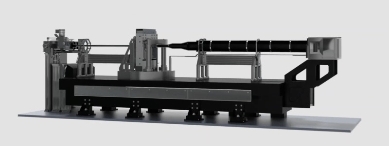
The Axion T2000 is a unique X-ray metrology solution for vertical memory chip manufacturing that uses CD-SAXS (critical dimension small angle X-ray scattering) technology. A high flux source produces X-rays that travel through custom optics and then transmit through the wafer, which is mounted vertically in a stage. The X-rays interact with the memory device structures on the wafer, creating diffraction patterns that are imaged by a high-efficiency detector. The stage, with industry-leading dynamic range, precisely rotates the wafer so that the X-rays pass through at several different angles of incidence and azimuths. The resulting set of diffraction images is encoded with 3D geometrical information. KLA’s industry-leading AcuShape modeling software extracts complex shape profile information from these images, including the subtle shape variations that can affect memory chip functionality or performance. With these innovations, the Axion T2000 non-destructively produces the dimensional metrology data needed to help memory manufacturers optimize, monitor and control key process steps inline.

With multiple systems in operation at leading memory manufacturers, the Axion T2000 joins KLA’s family of advanced metrology systems in providing precise measurement of complex parameters for 3D NAND and DRAM manufacturers. Covering the full range of metrology applications from early R&D to volume production, KLA’s comprehensive metrology portfolio produces information that drives faster ramp, improved device quality, and higher production yield.

.jpg)
