Researchers from Skoltech and their colleagues in Russia and Spain have reported a proof-of-concept demonstration of a new radiation-safe method for mapping the internal structure and stress distribution in samples of materials at the nanoscale, with a resolution about 100 times higher than that of the currently available techniques: X-ray and neutron tomography. The team believes that its 3D stress nanotomography could eventually become a standard metrological technique for nanotechnology.
The properties of materials change under stress, and this has been exploited by human technology from ancient smiths forging metalware to prestressed concrete enabling the existence of some of the tallest buildings and largest bridges of our time. Now, engineers working on ultrasmall devices could also benefit from stressed materials in ways many of which are hard to conceive ahead of time. But there’s a caveat.
“To exploit stressed materials, you need a way to precisely tell how stress is distributed on the inside, and hence how the properties will vary across the sample,” study co-author and Skoltech Professor Nikolai Brilliantov explained. “This involves the 3D mapping of internal inhomogeneities, such as dense spots and cavities, which is usually accomplished with tomography.”
Same as with the familiar CT scan, tomography in general denotes methods for investigating the internal structure of an object slice by slice, without damaging it. The object is illuminated from many angles, with the passing radiation detected on the opposite side. This is repeated for many separate planes ‘cutting’ through the sample, resulting in a series of 2D ‘slices,’ later combined into a complete 3D model via some rather sophisticated mathematics.
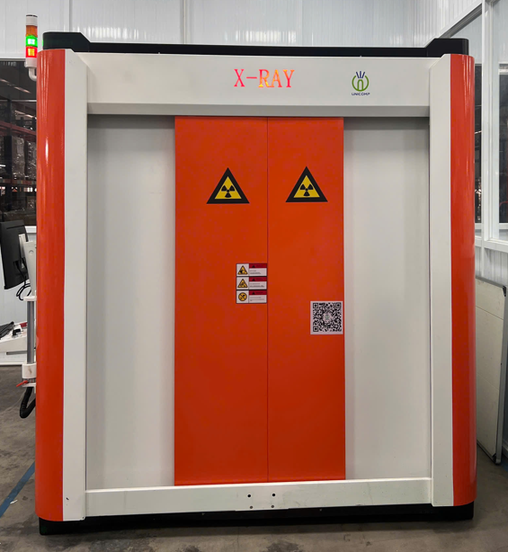
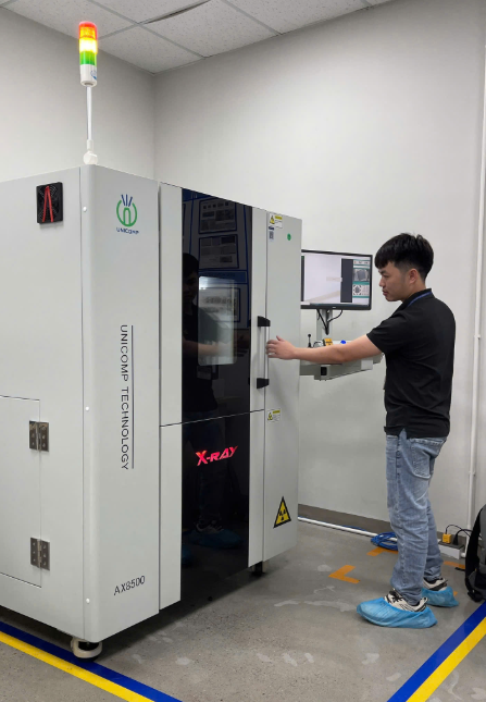
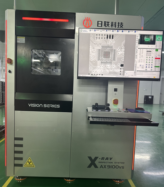
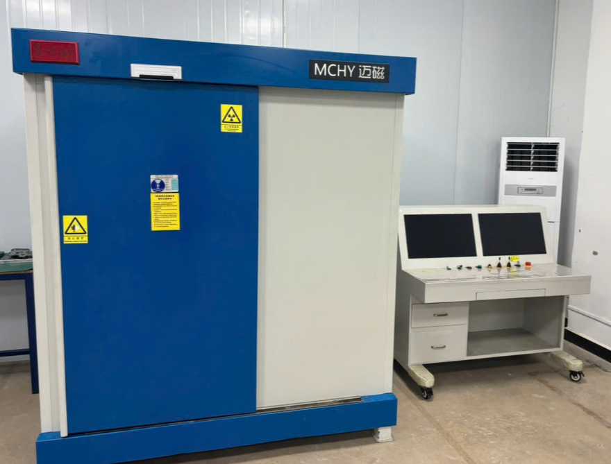
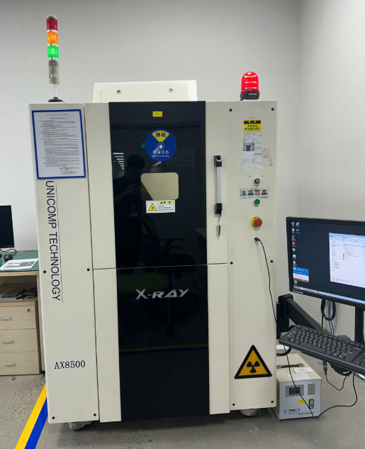
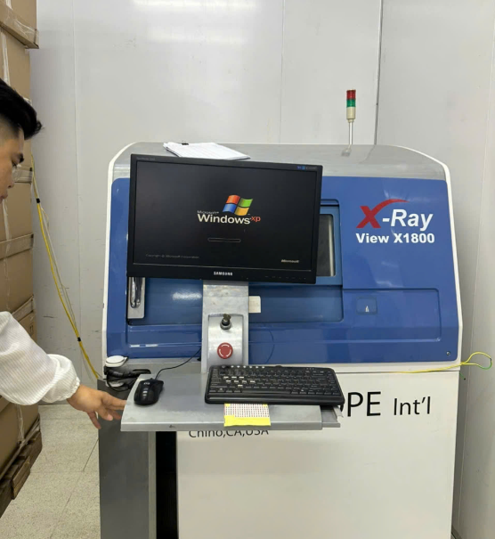
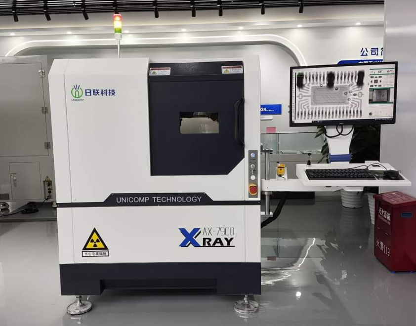
The two kinds of tomography that could potentially help in stress-aware nanotechnology rely on X-rays and neutrons to screen the sample. Both entail direct radiation hazards for the personnel during operation and induce ‘secondary’ radioactivity in the workplace. The process also runs the risk of damaging the sample due to its repeated exposure to high-energy rays. Most importantly, the sensors used to detect the passing radiation have grain sizes that are too large. That is, they make it impossible to obtain truly nanoresolved images. As for transmission electron microscopy, it has the principal limitation that the samples should be extremely thin slices.
“We address all of these shortcomings and open the way for future nanotechnology applications by demonstrating a new kind of tomography that yields about 100 times higher resolution and does not use hazardous radiation, avoiding both the health issues and damage to the sample,” Brilliantov said.
At the heart of stress nanotomography is the phenomenon of piezoelectricity: Some materials accumulate electric charge when exposed to mechanical stress. Known as piezoelectric materials, these include a subclass called ferroelectrics, for which the stress-to-electricity conversion is particularly pronounced. The latter were used as samples for analysis in the study, but according to the team, the new stress tomography should work on other solid materials, too, but in that case ferroelectrics would have to play an auxiliary role.
Here is how the proof-of-concept system works. A metal needle slides across the surface of a ferroelectric material many times over in different directions and pressing down with varying force. All the while, the varying electric field produced by the material under pressure is recorded as electrical current pulses induced in the metal tip. Since the measured electric field is directly related to the material’s local density at any given point, it is possible to reconstruct the internal structure of the sample and its stress distribution from those data.
Reconstructing the 3D structure from the collected tomography data is known as solving the inverse problem, and it is far from trivial. “This is the first time the inverse problem has been solved for a piezoelectric material,” study co-author and Skoltech Research Scientist Gleb Ryzhakov commented. “First, we had to create a model that explains what actually happens in terms of physics as the metal tip slides across the sample surface. Second, we came up with the mathematical tools for solving the inverse problem. Third, we developed an applied software suite for recovering tomography images from the recorded current signals.”
According to the team, one of the ways to enhance the technique in the future will be by expanding the range of materials whose inner makeup can be studied to include nonpiezoelectric solids. “It’s a matter of sophisticated engineering: Provided we can manufacture a very thin but durable piezoelectric film, we could lay it between the metal tip of the tomograph and the sample. Theoretically, it should then work on arbitrary materials, but the electric field measurements will have to be very precise,” Ryzhakov added.
“We expect that in the future, such stress nanotomography will be routinely incorporated in numerous stress-based nanotechnologies,” Brilliantov concluded.
The study came out in the Journal of the Mechanics and Physics of Solids.
Skoltech is a private international university located in Russia. Established in 2011 in collaboration with the Massachusetts Institute of Technology (MIT).

