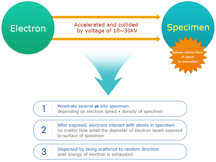
Interaction between electron and solid

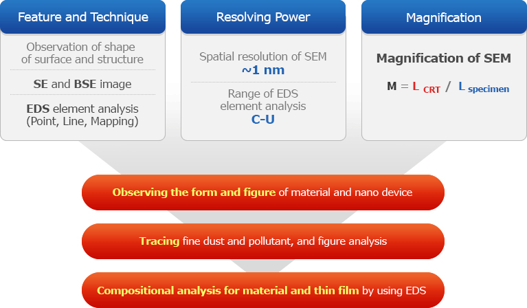
SEM Overview
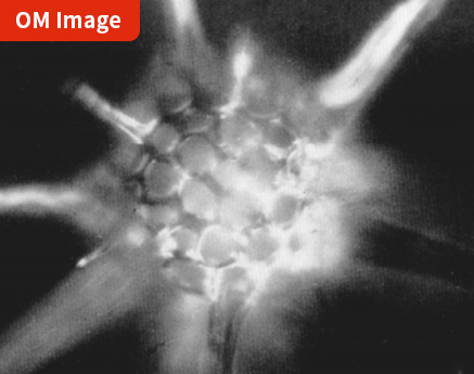
Optical Microscope
Low resolving power, Low depth of focus

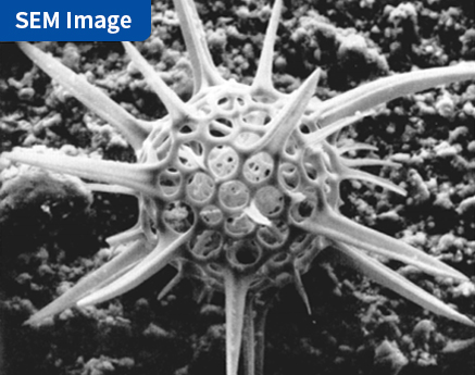
Scanning Electron Microscope
High resolving power, High depth of focus

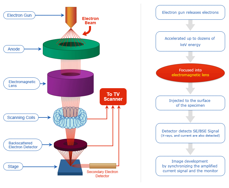
Overview of SEM analysis : Device

SE (Secondary Electron)
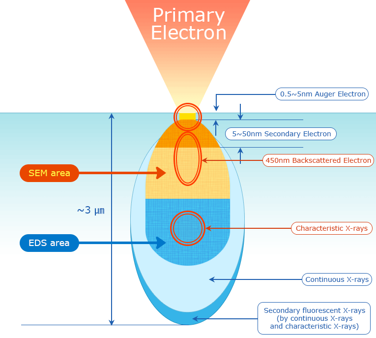
Electron having energy less than 50eV generated in the specimen by inelastic collision of electronic beam and the specimen when incident electron beam collided with the specimen
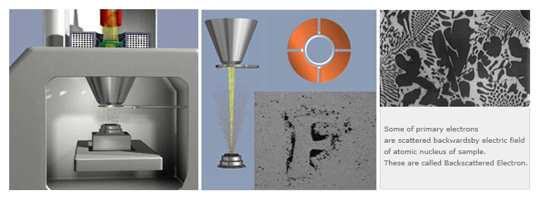
BSE (Backscattered Electron)
Electron emitted backwards when incident electron beam collided with the specimen
SEM Overview

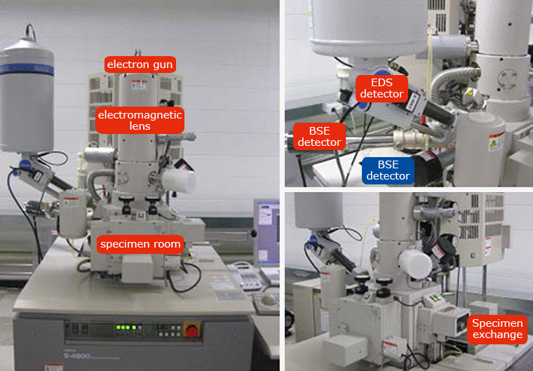
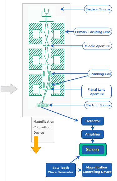
Overview of SEM analysis : Device

Electron Lens
1) How small the size of electron beam shot into specimen can get is the key of high resolution of SEM
2) ELECRTON LENS
–Condenser Lens
- Reduces crossover made up in Electron gun
- Controls Spot size
–Objective Lens
- Changes location of Prove crossover depending on optic axis
- Focuses image
- Generating electron ray
- Lens system controlling electron ray
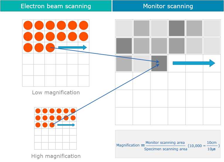
- Scan Coil deciding magnification by deciding scanning area on the specimen
- Stigmator eliminating astigmatism
- Detector collecting Signal gained from specimen
- CRT showing information gained from Detector

Principle of magnification of SEM

Interaction volume and signal


SE / BSE Detector

SE(Secondary Electron)
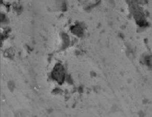
SE forms image with information from bump reflection / generally used to compose the overall image by observing the surface shape.

BSE(Backscattered Electron)
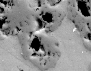
Images are formed by the component(atomic number) composing the specimen and 발생계수 increases according to the increase of atomic number
SE (Secondary Electron) Detector

-
Secondary Electron ▷Electron generated on the surface of specimen by the energy gained from inelastic collision with beam electron
-
Generated by interaction of activated beam electron and weakly vibrating metal
-
Only small amount of kinetic energy is transferred to secondary electron because the amount of energy in beam electron is very small compared to the electron of specimen.
-
Most of SEMs are installed Everhart-Thomley (E-T) Detector.
Photons are generated when activated electrons collide with Scintillator. Then, they move into photomultiplier tube by total reflection in optical waveguide. Photons can go through vacuum and quartz window because they are in the form of light. Photons attract current from both poles, collect and go back to current at detectable point.
BSE (Backscattered Electron) Detector

Electrons sent to sample and shot out are scattered to various directions. These are divided into elastic or inelastic scattering of electron.
-
Elastic scattering of primary electron; Scattered electrons change momentum but energy doesn’t change or change within 1eV. Because P=mv and m doesn’t change, only the direction of speed vector changes. Scattering angle is 0-180° and typically 5°
-
Elastic scattering is generated between negative electron and positive atomic nucleus.
-
Some electrons have large scattering angle to be shot outside the sample and these are backscattered electrons.
-
Lighter part of image is coper and darker part is aluminium in the image by BSE detector
-
Energy during inelastic scattering is transferred to electrons around atom and kinetic energy in activated electrons is reduced.
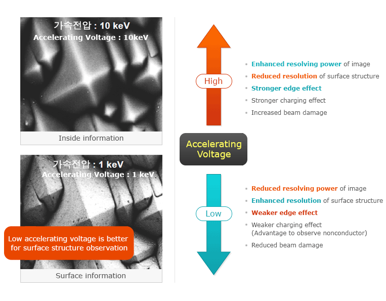
Image change depending on Accelerating Voltage

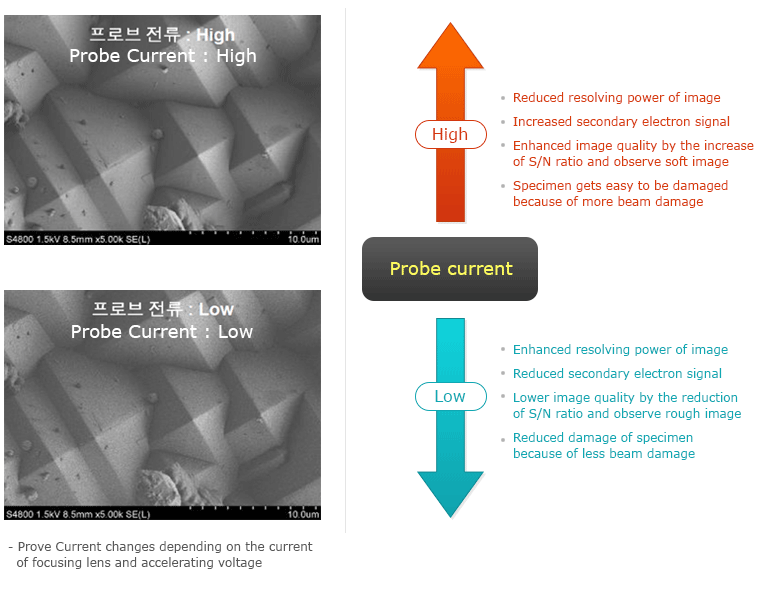
Image change depending on Probe Current

Image distortion depending on Astigmatism

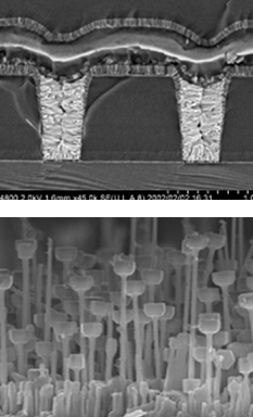
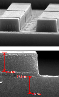
Observation by SEM
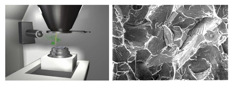
Observation of surface image

Observation of cross-section structure

Thickness
measurement

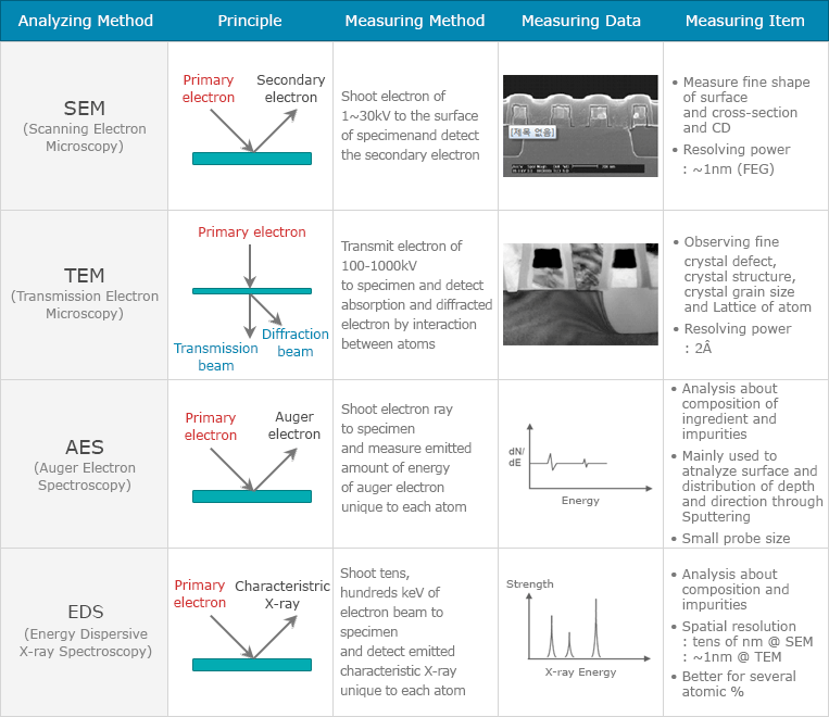
Conclusion. Principle and feature of electron beam analyzing technique

Reference
-
Principle and Application of electron microscope
-
Analysis of SEM and X-ray microanalysis


